Build an ATS-Friendly
PCB Design Engineer Resume
That Gets Interviews
A PCB Design Engineer translates complex electrical design requirements into tangible printed circuit layouts, iterating through phases of design and validation. They create schematics and layouts using specialized software, ensuring adherence to design rules and industry standards. These engineers collaborate…
PCB Design Engineer Resume Templates
Modern Professional
Use Template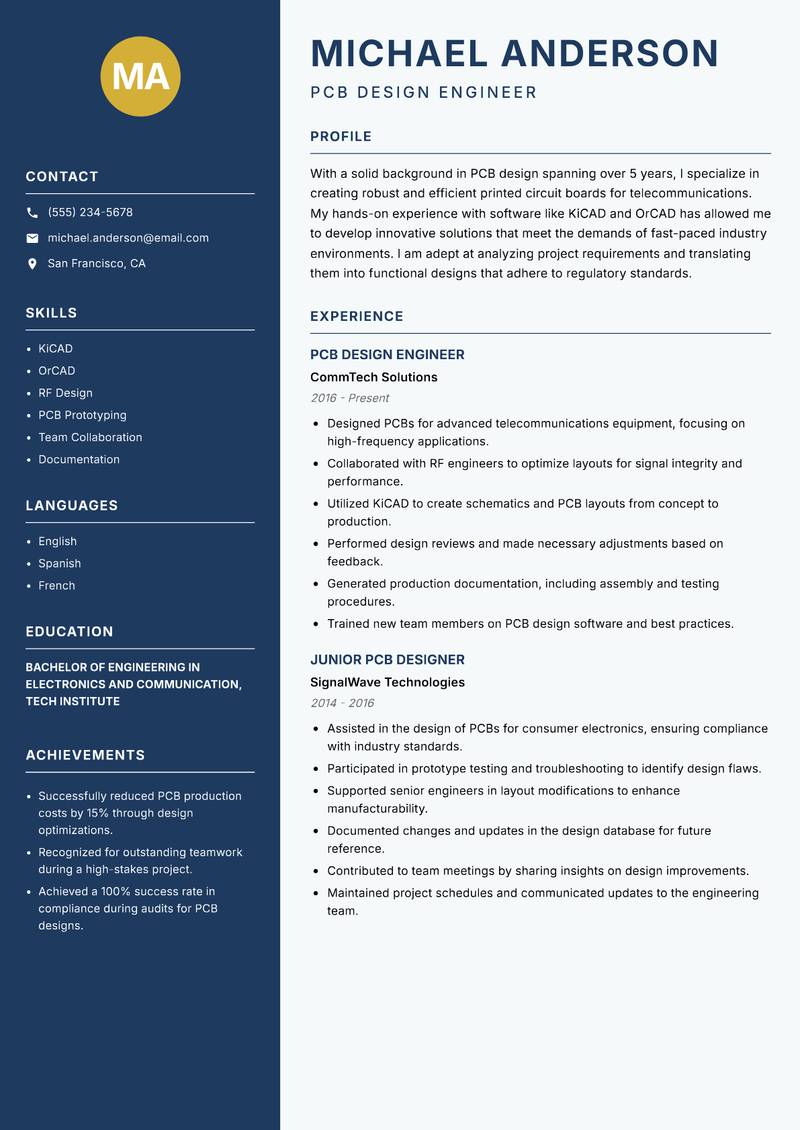
Classic Clean
Use Template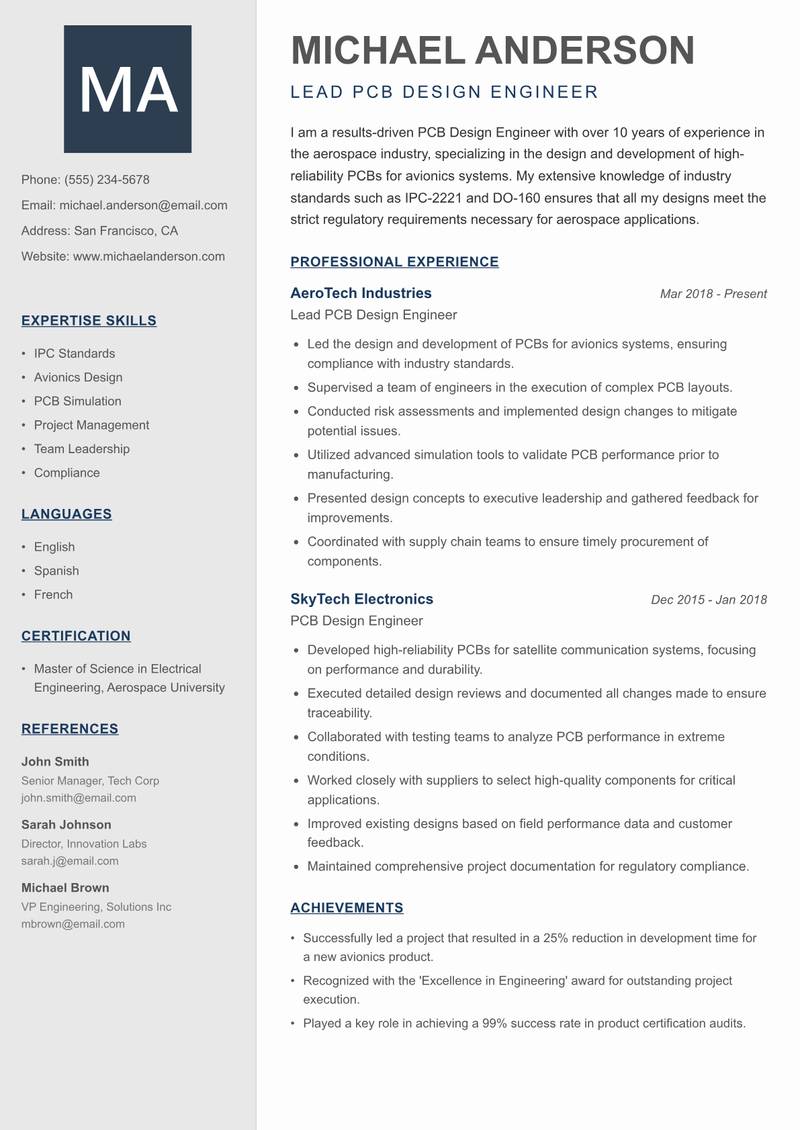
Creative Minimal
Use Template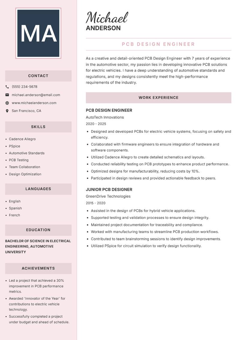
Executive
Use Template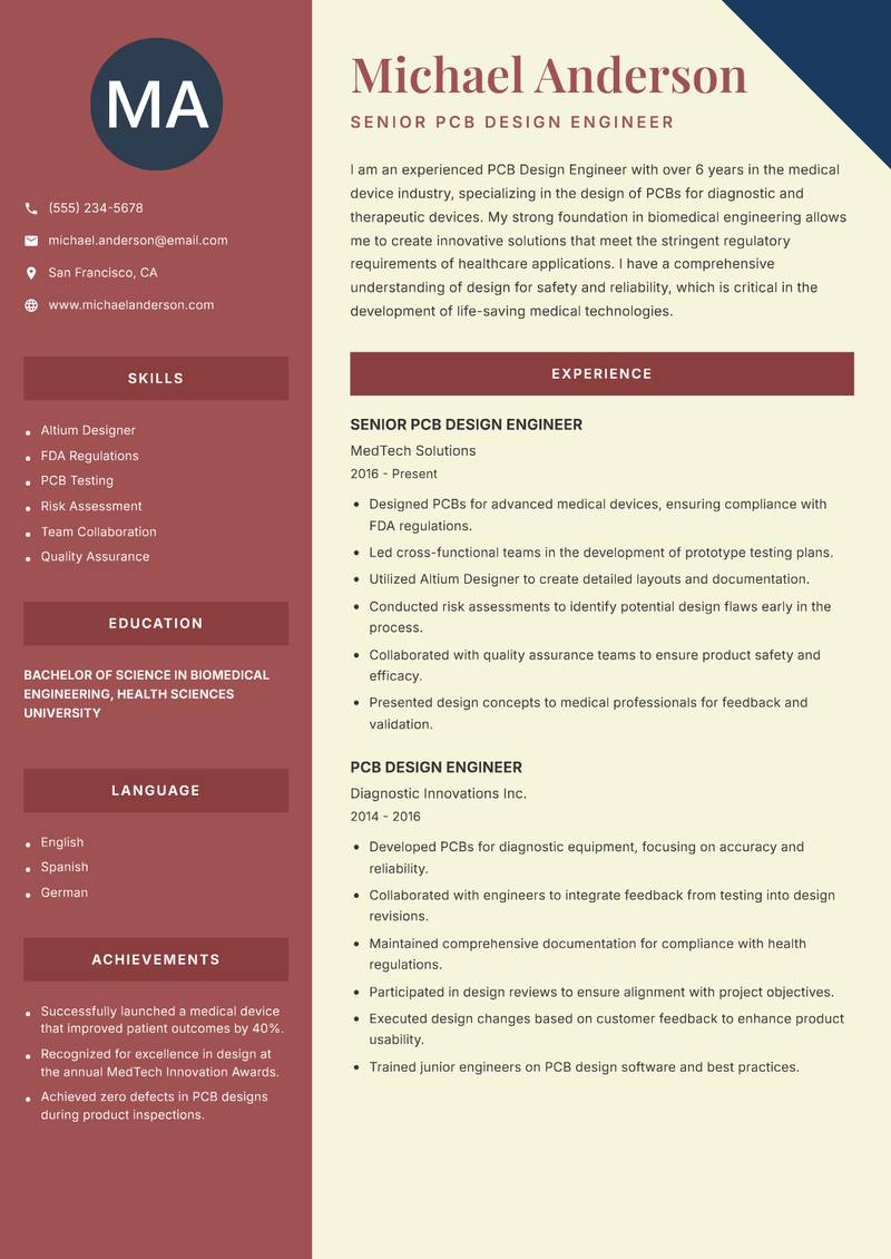
Two Column
Use Template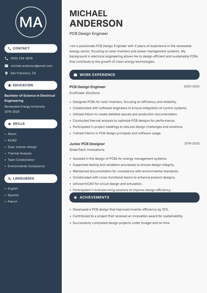
Compact
Use Template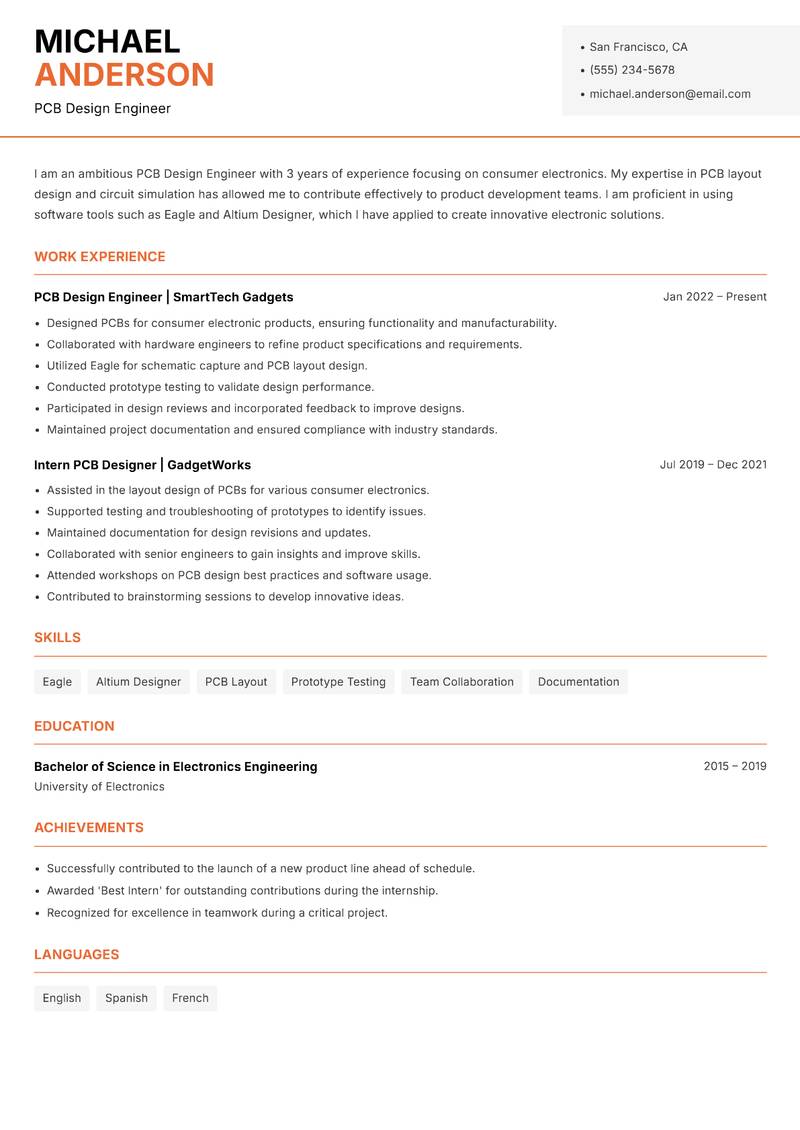
Modern Professional
Use Template7 Real PCB Design Engineer Resume Examples
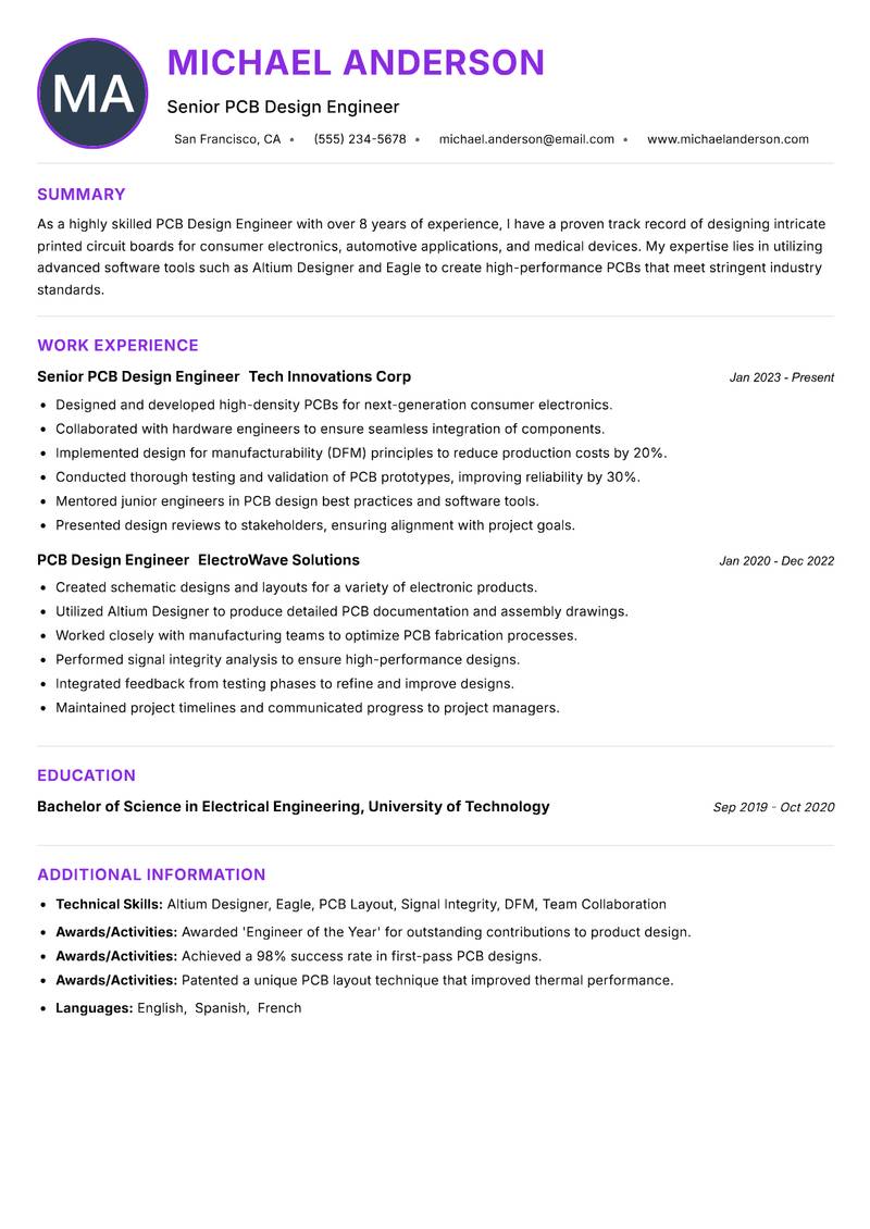
Senior PCB Design Engineer with 8+ Years Experience
Summary: As a highly skilled PCB Design Engineer with over 8 years of experience, I have a proven track record of designing intricate printed circuit boards for consumer electronics, automotive applications, and medical devices. My expertise lies in utilizing advanced software tools such as Altium Designer and Eagle to create high-performance PCBs that meet stringent industry standards. I have successfully led projects from concept through production, ensuring that designs are optimized for manufacturability and reliability. My strong analytical skills enable me to troubleshoot complex issues, while my attention to detail ensures that every design is executed with precision. I am passionate about keeping up with the latest technology trends and continuously seek opportunities to enhance my skills. I thrive in collaborative environments and have effectively communicated with cross-functional teams to deliver projects on time and within budget. My commitment to quality and innovation in PCB design has consistently resulted in the successful launch of products that exceed customer expectations.
Description:
- Designed and developed high-density PCBs for next-generation consumer electronics.
- Collaborated with hardware engineers to ensure seamless integration of components.
- Implemented design for manufacturability (DFM) principles to reduce production costs by 20%.
- Conducted thorough testing and validation of PCB prototypes, improving reliability by 30%.
- Mentored junior engineers in PCB design best practices and software tools.
- Presented design reviews to stakeholders, ensuring alignment with project goals.
🏆 Key Achievements
PCB Design Engineer with 5+ Years Experience
Summary: With a solid background in PCB design spanning over 5 years, I specialize in creating robust and efficient printed circuit boards for telecommunications. My hands-on experience with software like KiCAD and OrCAD has allowed me to develop innovative solutions that meet the demands of fast-paced industry environments. I am adept at analyzing project requirements and translating them into functional designs that adhere to regulatory standards. My role often involves collaboration with multidisciplinary teams to ensure that all aspects of the PCB design process are aligned with project goals. I am committed to continuous learning and regularly attend workshops to stay current with industry advancements. My analytical mindset and problem-solving abilities have been key in optimizing designs for performance and cost efficiency. As a PCB Design Engineer, I am passionate about contributing to the development of cutting-edge technologies that improve communication systems worldwide.
Description:
- Designed PCBs for advanced telecommunications equipment, focusing on high-frequency applications.
- Collaborated with RF engineers to optimize layouts for signal integrity and performance.
- Utilized KiCAD to create schematics and PCB layouts from concept to production.
- Performed design reviews and made necessary adjustments based on feedback.
- Generated production documentation, including assembly and testing procedures.
- Trained new team members on PCB design software and best practices.
🏆 Key Achievements
Lead PCB Design Engineer with 10+ Years Experience
Summary: I am a results-driven PCB Design Engineer with over 10 years of experience in the aerospace industry, specializing in the design and development of high-reliability PCBs for avionics systems. My extensive knowledge of industry standards such as IPC-2221 and DO-160 ensures that all my designs meet the strict regulatory requirements necessary for aerospace applications. I have a passion for innovation and am always looking for ways to incorporate new technologies into my designs. My experience includes leading cross-functional teams through the entire product lifecycle, from initial concept to testing and production. I pride myself on my strong project management skills, which have enabled me to complete projects on time and within budget. My ability to communicate complex technical information to non-technical stakeholders has been instrumental in ensuring project alignment and success. I am committed to continuous improvement and actively seek feedback to enhance my design processes and outcomes.
Description:
- Led the design and development of PCBs for avionics systems, ensuring compliance with industry standards.
- Supervised a team of engineers in the execution of complex PCB layouts.
- Conducted risk assessments and implemented design changes to mitigate potential issues.
- Utilized advanced simulation tools to validate PCB performance prior to manufacturing.
- Presented design concepts to executive leadership and gathered feedback for improvements.
- Coordinated with supply chain teams to ensure timely procurement of components.
🏆 Key Achievements
PCB Design Engineer with 7+ Years Experience
Summary: As a creative and detail-oriented PCB Design Engineer with 7 years of experience in the automotive sector, my passion lies in developing innovative PCB solutions for electric vehicles. I have a deep understanding of automotive standards and regulations, and my designs consistently meet the high-performance requirements of the industry. Proficient in using Cadence Allegro and PSpice, I have successfully contributed to several high-profile projects that focus on enhancing vehicle safety and performance. My collaborative approach allows me to work effectively with software and hardware teams to ensure that our designs are not only functional but also manufacturable. I am dedicated to professional development and actively seek opportunities to learn about emerging technologies in the automotive field. My commitment to quality and efficiency has led to the successful launch of multiple products, driving forward the future of mobility.
Description:
- Designed and developed PCBs for electric vehicle systems, focusing on safety and efficiency.
- Collaborated with firmware engineers to ensure integration of hardware and software components.
- Utilized Cadence Allegro to create detailed schematics and layouts.
- Conducted reliability testing on PCB prototypes to enhance product performance.
- Optimized designs for manufacturability, reducing costs by 10%.
- Participated in design reviews and provided actionable feedback to peers.
🏆 Key Achievements
Senior PCB Design Engineer with 6+ Years Experience
Summary: I am an experienced PCB Design Engineer with over 6 years in the medical device industry, specializing in the design of PCBs for diagnostic and therapeutic devices. My strong foundation in biomedical engineering allows me to create innovative solutions that meet the stringent regulatory requirements of healthcare applications. I have a comprehensive understanding of design for safety and reliability, which is critical in the development of life-saving medical technologies. I am proficient in using software such as Altium Designer and Mentor Graphics, and my designs have consistently resulted in successful product launches. My ability to communicate effectively with cross-functional teams ensures that all project requirements are met, and I am dedicated to maintaining high standards of quality throughout the design process. I am passionate about contributing to advancements in healthcare technology and am committed to continuous professional development.
Description:
- Designed PCBs for advanced medical devices, ensuring compliance with FDA regulations.
- Led cross-functional teams in the development of prototype testing plans.
- Utilized Altium Designer to create detailed layouts and documentation.
- Conducted risk assessments to identify potential design flaws early in the process.
- Collaborated with quality assurance teams to ensure product safety and efficacy.
- Presented design concepts to medical professionals for feedback and validation.
🏆 Key Achievements
PCB Design Engineer with 4+ Years Experience
Summary: I am a passionate PCB Design Engineer with 4 years of experience in the renewable energy sector, focusing on solar inverters and power management systems. My background in electrical engineering allows me to design efficient and sustainable PCBs that contribute to the growth of clean energy technologies. I am skilled in using PCB design tools such as Altium and KiCAD, and I have a strong understanding of environmental regulations and standards. My approach to design emphasizes sustainability while ensuring performance and reliability. I thrive in collaborative environments and have a proven ability to communicate technical information to diverse audiences. I am committed to staying current with industry trends and continuously seek opportunities to improve my skills and knowledge in renewable energy technologies. My dedication to innovation has led to successful product developments that align with the global push for sustainable solutions.
Description:
- Designed PCBs for solar inverters, focusing on efficiency and reliability.
- Collaborated with software engineers to ensure integration of control systems.
- Utilized Altium to create detailed layouts and production documentation.
- Conducted thermal analysis to optimize PCB designs for performance.
- Participated in project meetings to discuss design challenges and solutions.
- Trained interns in PCB design principles and software usage.
🏆 Key Achievements
PCB Design Engineer with 3+ Years Experience
Summary: I am an ambitious PCB Design Engineer with 3 years of experience focusing on consumer electronics. My expertise in PCB layout design and circuit simulation has allowed me to contribute effectively to product development teams. I am proficient in using software tools such as Eagle and Altium Designer, which I have applied to create innovative electronic solutions. My approach emphasizes collaboration and communication, ensuring that I work closely with other engineers to meet project objectives. I have a strong understanding of the entire product lifecycle and am dedicated to producing high-quality designs that are both functional and manufacturable. I am eager to learn and grow in the field of electronics, and I consistently strive to enhance my technical skills and knowledge.
Description:
- Designed PCBs for consumer electronic products, ensuring functionality and manufacturability.
- Collaborated with hardware engineers to refine product specifications and requirements.
- Utilized Eagle for schematic capture and PCB layout design.
- Conducted prototype testing to validate design performance.
- Participated in design reviews and incorporated feedback to improve designs.
- Maintained project documentation and ensured compliance with industry standards.
🏆 Key Achievements
Key Skills for PCB Design Engineer
ATS Optimization Tips
Increase your chances of getting hired
Use Standard Headings
Use common section titles like Experience, Skills, etc.
Include Keywords
Add role-specific keywords from the job description
Keep it Simple
Avoid complex tables, images and graphics
Save in Right Format
Use PDF format unless otherwise specified
PCB Design Engineer Salary Insights
Average Salary
$95,000
per year
Salary Range
$70,000 - $120,000
per year
Top Paying Cities
Los Angeles, Seattle, Houston, Dallas, Boston
Source: Glassdoor, Payscale, Indeed (Updated June 2025)
Everything you need to write a great PCB Design Engineer resume
Strong Action Verbs to Use
Resume Writing Tips
- →Highlight specific PCB design software proficiency in your resume.
- →Include examples of successful project outcomes in your past work history.
- →Clearly demonstrate your understanding of PCB manufacturing processes.
- →Incorporate quantifiable achievements, like reducing design cycle time or improving yield.
- →Tailor your resume with keywords specific to the jobs you're applying for to bypass ATS filters.
Common Mistakes to Avoid
- ✕Overgeneralizing experience without specifying tools or techniques used.
- ✕Failing to include relevant certifications or industry standards compliance.
- ✕Listing duties instead of achievements or unique contributions to projects.
- ✕Neglecting to mention collaboration experiences with other teams like mechanical or firmware design.
ATS Keywords for PCB Design Engineer
PCB Design Engineer Career Path
Relevant Certifications
Career Progression
Entry-Level PCB Design Engineer
Typically involves working under the supervision of senior engineers, assisting in schematic designs, and performing basic simulations.
Mid-Level PCB Design Engineer
At this stage, engineers take on complex projects, lead small teams, and start interfacing with other disciplines such as mechanical and software engineering.
Senior PCB Design Engineer
Responsible for overseeing all PCB project phases from conception to production, including mentoring junior engineers and collaborating with cross-functional teams.
Lead PCB Design Engineer
Manages multiple project timelines, coordinates design reviews, and serves as the primary technical authority on PCB issues.
PCB Engineering Manager
Oversees the PCB design department, develops strategic initiatives, and liaises with upper management regarding budget and resource allocation.
PCB Design Engineer Interview Questions
Can you explain your experience with using CAD tools for PCB design? +
Be specific about the software you have used (like Altium Designer or OrCAD) and describe a project where you applied these tools.
How do you approach ensuring signal integrity in your designs? +
Discuss specific techniques such as routing strategies or impedance control.
What is your process for selecting components for a PCB project? +
Mention factors like cost, availability, and functionality in relation to the end application.
Have you ever faced a design challenge? How did you resolve it? +
Provide a concrete example that demonstrates problem-solving skills specific to PCB complexities.
How do you handle design reworks or changes requested by clients? +
Explain your method for tracking changes and communicating with stakeholders to ensure smooth project management.
What strategies do you use for thermal management in PCB design? +
Discuss specific methods or technologies you've utilized to manage heat dissipation.
How do you ensure compliance with industry standards and regulations in your PCB designs? +
Talk about familiarity with standards such as IPC or IEEE and how you integrate them into your workflow.
About the PCB Design Engineer Role
A PCB Design Engineer translates complex electrical design requirements into tangible printed circuit layouts, iterating through phases of design and validation. They create schematics and layouts using specialized software, ensuring adherence to design rules and industry standards. These engineers collaborate closely with software and electrical teams, bridging gaps between circuit design and real-world applications.
Frequently Asked Questions
View all →What is the primary software used by PCB Design Engineers? +
Commonly used software includes Altium Designer, OrCAD, and KiCad for schematic capture and PCB layout.
What types of projects do PCB Design Engineers typically work on? +
Projects can range from automotive electronics and consumer devices to complex telecommunications equipment and medical devices.
How important is teamwork in PCB design? +
Teamwork is crucial as PCB Design Engineers must collaborate with electrical engineers, mechanical engineers, and product managers to ensure cohesive development.
What industries employ PCB Design Engineers? +
PCB Design Engineers are employed across various industries including consumer electronics, aerospace, automotive, telecommunications, and medical devices.
Are there any online resources for PCB Design Engineers to improve their skills? +
Yes, platforms like Coursera, edX, and specific PCB design forums offer valuable courses and community support for skill enhancement.
How often do PCB Design Engineers need to update their skills? +
Due to rapid advancements in technology, continuous learning is essential, with a focus on updating software skills and staying informed about industry standards.
What is the most challenging part of being a PCB Design Engineer? +
One significant challenge is balancing design complexity with manufacturability and cost-effectiveness while optimizing for performance and reliability.
More Resume Examples You Might Like
Related Career Paths
Other roles candidates for PCB Design Engineer positions often also consider.
Will this PCB Design Engineer resume pass the ATS scan?
Upload it and get an instant AI-scored compatibility check with specific fixes.
Check My Resume →
Pair it with a matching cover letter
AI drafts a first version from your job title and strengths — edit it live, then download the PDF.
Write My Cover Letter →
Written by Nohaya Career Team
Reviewed by HR Professionals · Updated June 2025
Ready to Build Your Perfect Resume?
Choose from 1000+ professional templates and land your dream job.
Create My Resume Now