Build an ATS-Friendly
Nanophotonics Engineer Resume
That Gets Interviews
Nanophotonics Engineers develop cutting-edge technologies that manipulate light at the nanoscale, often leading to enhanced performance in telecommunications, imaging, and sensing applications. These engineers create and analyze nanostructured materials and devices, applying their knowledge to address real-world…
Nanophotonics Engineer Resume Templates
Modern Professional
Use Template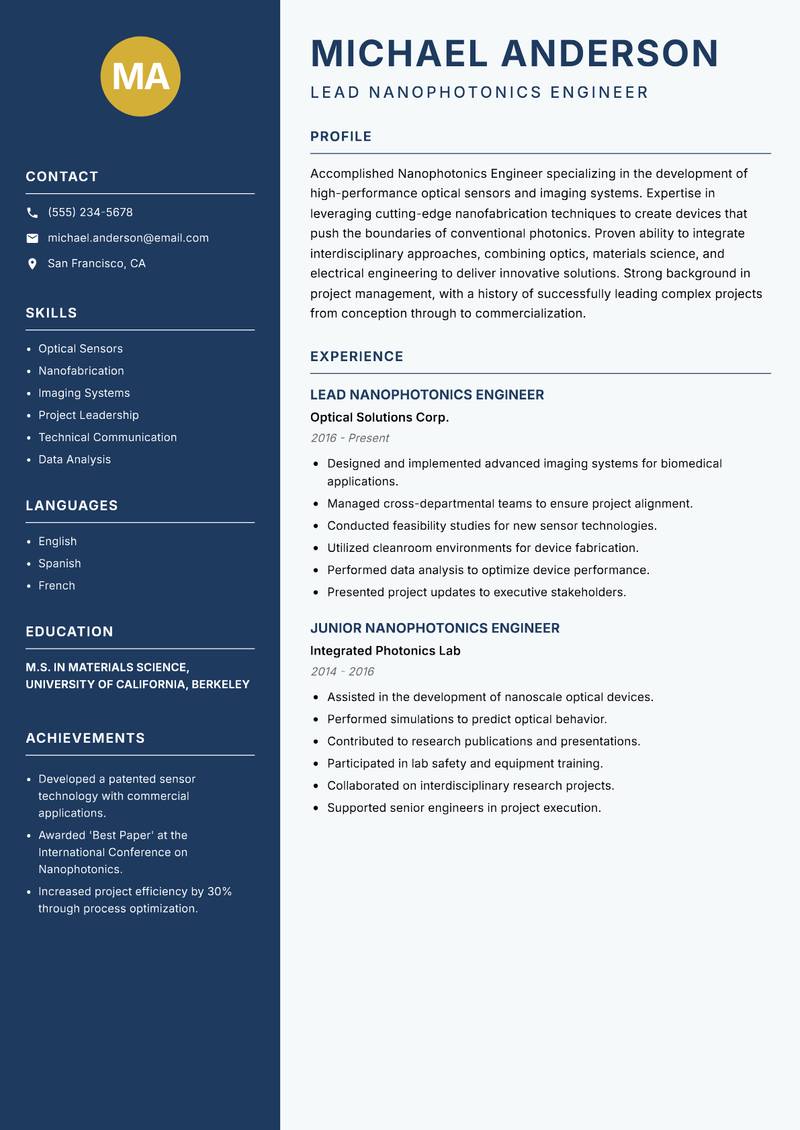
Classic Clean
Use Template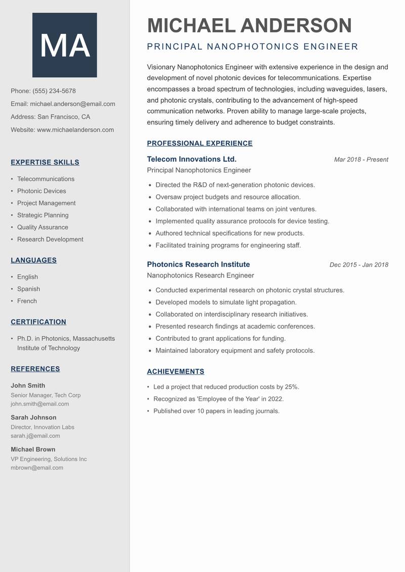
Creative Minimal
Use Template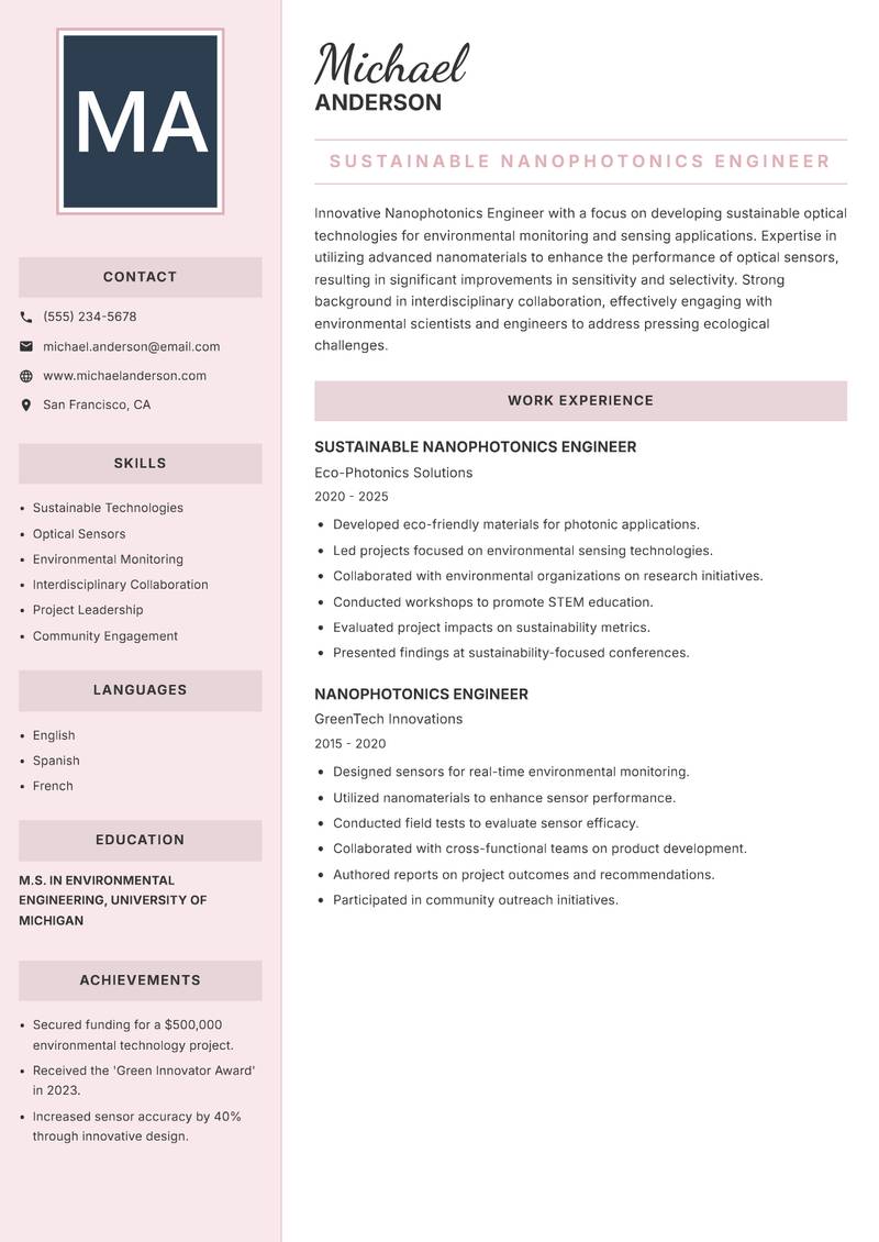
Executive
Use Template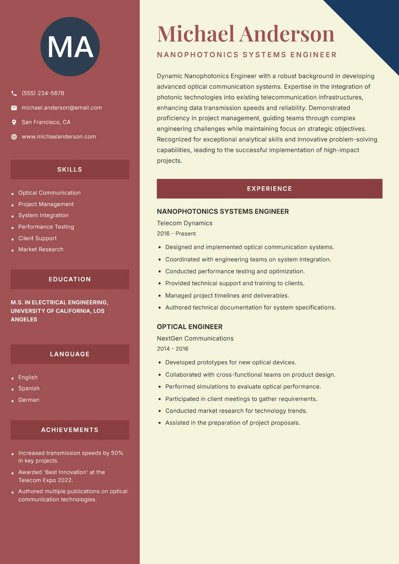
Two Column
Use Template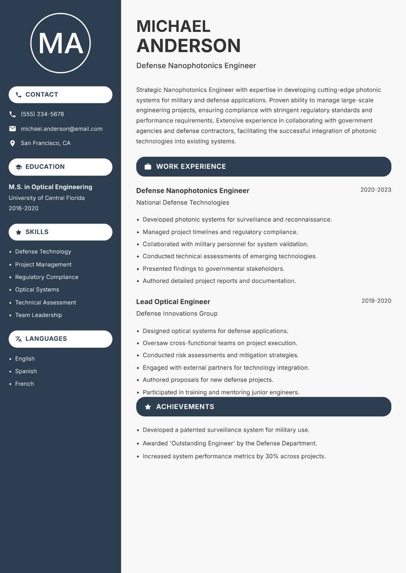
Compact
Use Template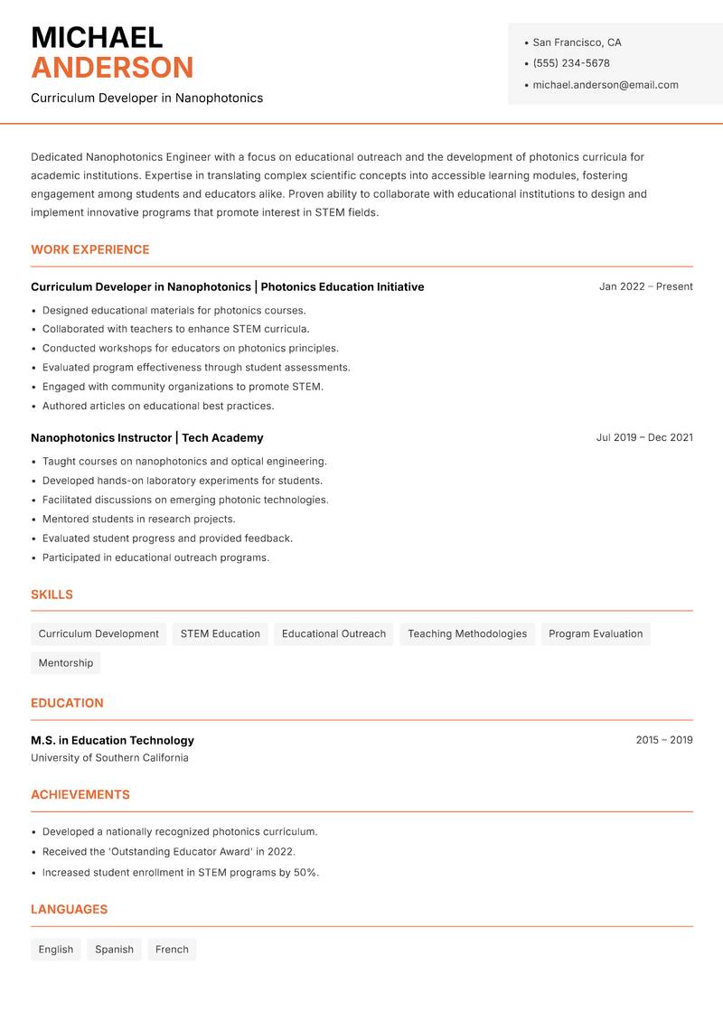
Modern Professional
Use Template7 Real Nanophotonics Engineer Resume Examples
Senior Nanophotonics Engineer with 8+ Years Experience
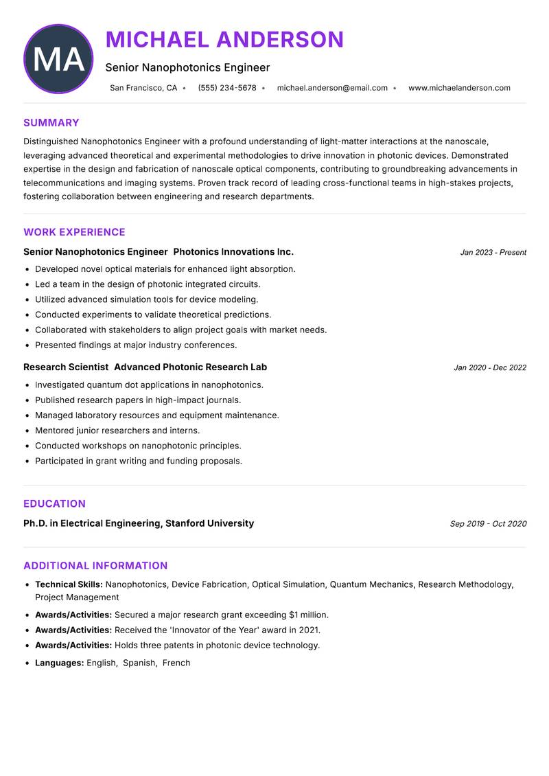
Summary: Distinguished Nanophotonics Engineer with a profound understanding of light-matter interactions at the nanoscale, leveraging advanced theoretical and experimental methodologies to drive innovation in photonic devices. Demonstrated expertise in the design and fabrication of nanoscale optical components, contributing to groundbreaking advancements in telecommunications and imaging systems. Proven track record of leading cross-functional teams in high-stakes projects, fostering collaboration between engineering and research departments. Adept at employing state-of-the-art characterization techniques to evaluate device performance, ensuring alignment with stringent industry standards. Committed to advancing the field of nanophotonics through continuous research and development, with a focus on sustainability and energy efficiency. Recognized for contributions to peer-reviewed journals and international conferences, setting benchmarks for future research. Possesses a comprehensive understanding of market trends, positioning the organization as a leader in technological innovation.
Description:
- Developed novel optical materials for enhanced light absorption.
- Led a team in the design of photonic integrated circuits.
- Utilized advanced simulation tools for device modeling.
- Conducted experiments to validate theoretical predictions.
- Collaborated with stakeholders to align project goals with market needs.
- Presented findings at major industry conferences.
🏆 Key Achievements
Lead Nanophotonics Engineer with 5+ Years Experience
Summary: Accomplished Nanophotonics Engineer specializing in the development of high-performance optical sensors and imaging systems. Expertise in leveraging cutting-edge nanofabrication techniques to create devices that push the boundaries of conventional photonics. Proven ability to integrate interdisciplinary approaches, combining optics, materials science, and electrical engineering to deliver innovative solutions. Strong background in project management, with a history of successfully leading complex projects from conception through to commercialization. Recognized for excellence in technical writing and communication, enabling clear dissemination of complex concepts to diverse audiences. Committed to fostering a culture of collaboration and knowledge sharing within teams. Actively engaged in the professional community, contributing to various technical committees and working groups.
Description:
- Designed and implemented advanced imaging systems for biomedical applications.
- Managed cross-departmental teams to ensure project alignment.
- Conducted feasibility studies for new sensor technologies.
- Utilized cleanroom environments for device fabrication.
- Performed data analysis to optimize device performance.
- Presented project updates to executive stakeholders.
🏆 Key Achievements
Principal Nanophotonics Engineer with 8+ Years Experience
Summary: Visionary Nanophotonics Engineer with extensive experience in the design and development of novel photonic devices for telecommunications. Expertise encompasses a broad spectrum of technologies, including waveguides, lasers, and photonic crystals, contributing to the advancement of high-speed communication networks. Proven ability to manage large-scale projects, ensuring timely delivery and adherence to budget constraints. Recognized for strategic thinking and problem-solving capabilities, enabling the identification of innovative solutions to complex engineering challenges. Strong advocate for sustainable practices in photonics, actively pursuing eco-friendly materials and processes. Engaged in continuous professional development, staying abreast of technological advancements and industry trends. A collaborative leader, committed to mentoring future engineers and fostering a culture of innovation.
Description:
- Directed the R&D of next-generation photonic devices.
- Oversaw project budgets and resource allocation.
- Collaborated with international teams on joint ventures.
- Implemented quality assurance protocols for device testing.
- Authored technical specifications for new products.
- Facilitated training programs for engineering staff.
🏆 Key Achievements
Sustainable Nanophotonics Engineer with 6+ Years Experience
Summary: Innovative Nanophotonics Engineer with a focus on developing sustainable optical technologies for environmental monitoring and sensing applications. Expertise in utilizing advanced nanomaterials to enhance the performance of optical sensors, resulting in significant improvements in sensitivity and selectivity. Strong background in interdisciplinary collaboration, effectively engaging with environmental scientists and engineers to address pressing ecological challenges. Demonstrated leadership in project execution, ensuring alignment with sustainability goals and regulatory standards. Recognized for contributions to community outreach programs aimed at promoting STEM education among underrepresented groups. Committed to continuous learning and adaptation to new technologies, fostering an agile approach to engineering challenges. A proactive advocate for diversity and inclusion within the engineering field.
Description:
- Developed eco-friendly materials for photonic applications.
- Led projects focused on environmental sensing technologies.
- Collaborated with environmental organizations on research initiatives.
- Conducted workshops to promote STEM education.
- Evaluated project impacts on sustainability metrics.
- Presented findings at sustainability-focused conferences.
🏆 Key Achievements
Nanophotonics Systems Engineer with 6+ Years Experience
Summary: Dynamic Nanophotonics Engineer with a robust background in developing advanced optical communication systems. Expertise in the integration of photonic technologies into existing telecommunication infrastructures, enhancing data transmission speeds and reliability. Demonstrated proficiency in project management, guiding teams through complex engineering challenges while maintaining focus on strategic objectives. Recognized for exceptional analytical skills and innovative problem-solving capabilities, leading to the successful implementation of high-impact projects. Committed to professional growth and continuous improvement, actively pursuing certifications and training in emerging technologies. A collaborative team player, fostering a positive work environment and encouraging knowledge exchange among peers. Passionate about contributing to the advancement of photonics in the telecommunications sector.
Description:
- Designed and implemented optical communication systems.
- Coordinated with engineering teams on system integration.
- Conducted performance testing and optimization.
- Provided technical support and training to clients.
- Managed project timelines and deliverables.
- Authored technical documentation for system specifications.
🏆 Key Achievements
Defense Nanophotonics Engineer with 8+ Years Experience
Summary: Strategic Nanophotonics Engineer with expertise in developing cutting-edge photonic systems for military and defense applications. Proven ability to manage large-scale engineering projects, ensuring compliance with stringent regulatory standards and performance requirements. Extensive experience in collaborating with government agencies and defense contractors, facilitating the successful integration of photonic technologies into existing systems. Recognized for exceptional leadership skills, guiding multidisciplinary teams through complex project lifecycles. Committed to fostering innovation and excellence within the engineering domain, continuously seeking opportunities for professional development and knowledge enhancement. A proactive communicator, adept at articulating complex technical concepts to diverse audiences, including non-technical stakeholders. Passionate about contributing to advancements in national security through innovative photonic solutions.
Description:
- Developed photonic systems for surveillance and reconnaissance.
- Managed project timelines and regulatory compliance.
- Collaborated with military personnel for system validation.
- Conducted technical assessments of emerging technologies.
- Presented findings to governmental stakeholders.
- Authored detailed project reports and documentation.
🏆 Key Achievements
Curriculum Developer in Nanophotonics with 6+ Years Experience
Summary: Dedicated Nanophotonics Engineer with a focus on educational outreach and the development of photonics curricula for academic institutions. Expertise in translating complex scientific concepts into accessible learning modules, fostering engagement among students and educators alike. Proven ability to collaborate with educational institutions to design and implement innovative programs that promote interest in STEM fields. Recognized for excellence in curriculum development and teaching methodologies, enhancing student comprehension and retention. Committed to lifelong learning and professional development, actively participating in workshops and conferences to stay abreast of educational trends and technologies. A passionate advocate for diversity in education, striving to create inclusive learning environments that empower all students.
Description:
- Designed educational materials for photonics courses.
- Collaborated with teachers to enhance STEM curricula.
- Conducted workshops for educators on photonics principles.
- Evaluated program effectiveness through student assessments.
- Engaged with community organizations to promote STEM.
- Authored articles on educational best practices.
🏆 Key Achievements
Key Skills for Nanophotonics Engineer
ATS Optimization Tips
Increase your chances of getting hired
Use Standard Headings
Use common section titles like Experience, Skills, etc.
Include Keywords
Add role-specific keywords from the job description
Keep it Simple
Avoid complex tables, images and graphics
Save in Right Format
Use PDF format unless otherwise specified
Nanophotonics Engineer Salary Insights
Average Salary
$116,500
per year
Salary Range
$83,000 - $150,000
per year
Top Paying Cities
Los Angeles, Seattle, Houston, Dallas, Boston
Source: Glassdoor, Payscale, Indeed (Updated July 2026)
Everything you need to write a great Nanophotonics Engineer resume
Strong Action Verbs to Use
Resume Writing Tips
- →Highlight specific projects that demonstrate your expertise in nanophotonics, focusing on key achievements and innovations.
- →Emphasize familiarity with industry-standard simulation and modeling tools relevant to nanostructured devices.
- →Showcase publications or patents in nanophotonics to underline your contribution to the field.
- →Detail your collaborative experiences with researchers or cross-departmental teams to illustrate teamwork skills in R&D environments.
- →Use technical language accurately but ensure clarity for non-technical stakeholders reviewing your resume.
Common Mistakes to Avoid
- ✕Listing generic engineering skills rather than specifying nanophotonic competencies like device fabrication capacity.
- ✕Failing to quantify achievements, such as efficiencies gained or performance metrics in devices developed.
- ✕Neglecting to include relevant workshops or conferences attended that enhance your credibility in nanotechnology.
- ✕Overlooking the importance of tailored keywords which might not be recognized by ATS for specialized roles in nanophotonics.
ATS Keywords for Nanophotonics Engineer
Nanophotonics Engineer Career Path
Relevant Certifications
Career Progression
Entry-Level Engineer
Assists in the design and testing of nanophotonic structures, learns about photonic simulations and fabrication techniques.
Mid-Level Nanophotonics Engineer
Leads projects in the development of nanostructured devices, conducting research to enhance device performance and efficiency.
Senior Engineer/Research Scientist
Oversees complex nanophotonics projects, guiding teams in advanced material characterization and device applications.
Manager of Nanotechnology Projects
Manages budgets, timelines, and personnel on nanophotonics research initiatives, liaising with external stakeholders and partners.
Director of Nanophotonics Research
Sets strategic direction for nanophotonics R&D, and collaborates with academia and industry leaders to push the boundaries of the field.
Nanophotonics Engineer Interview Questions
What are some common fabrication techniques used in creating nanophotonic devices? +
Discuss methods such as electron-beam lithography, nanoimprinting, or focused ion beam etching.
How do you approach the simulation of light behavior in nanostructures? +
Explain your experience with tools like COMSOL Multiphysics or Lumerical FDTD.
Can you describe a project where you improved the efficiency of a photonic device? +
Share specific metrics or results that demonstrate your impact.
What challenges do you foresee in scaling nanophotonic devices for commercial applications? +
Discuss potential fabrication challenges, cost implications, or market readiness.
How do you ensure that your designs are manufacturable? +
Reference design principles or collaboration with fabrication teams.
What role do you think materials play in advancing nanophotonics? +
Discuss specific materials like graphene or silicon photonics.
How do you stay updated on the latest developments in nanophotonics? +
Mention relevant journals, conferences, or professional organizations.
About the Nanophotonics Engineer Role
Nanophotonics Engineers develop cutting-edge technologies that manipulate light at the nanoscale, often leading to enhanced performance in telecommunications, imaging, and sensing applications. These engineers create and analyze nanostructured materials and devices, applying their knowledge to address real-world challenges like energy efficiency and medical diagnostics. Regular interactions with cross-functional teams, including physicists, material scientists, and product developers, enable the translation of theoretical concepts into practical solutions that meet both technical and market requirements.
Frequently Asked Questions
View all →What industries employ Nanophotonics Engineers? +
Nanophotonics Engineers work across telecom, healthcare, material sciences, and renewable energy sectors, where photonic devices are essential.
What educational background is required for a Nanophotonics Engineer? +
A bachelor's degree in optical engineering, materials science, or related fields is typically required, with advanced studies preferred.
What are some current trends in the field of nanophotonics? +
Trends include the development of quantum dots for displays, advancements in photonic integrated circuits, and improvements in sensing technologies.
Can Nanophotonics Engineers work in research labs? +
Absolutely, many Nanophotonics Engineers are involved in research and development within academic and government laboratories.
What programming languages are useful for Nanophotonics Engineers? +
Familiarity with MATLAB, Python, and C++ is beneficial for simulations and data analysis tasks in this role.
Are there opportunities for remote work as a Nanophotonics Engineer? +
While some tasks can be performed remotely, hands-on lab work and device fabrication often require being on-site.
What is the career outlook for Nanophotonics Engineers? +
The demand for Nanophotonics Engineers is expected to grow as more industries adopt nanotechnology solutions for various applications.
More Resume Examples You Might Like
Will this Nanophotonics Engineer resume pass the ATS scan?
Upload it and get an instant AI-scored compatibility check with specific fixes.
Check My Resume →
Pair it with a matching cover letter
AI drafts a first version from your job title and strengths — edit it live, then download the PDF.
Write My Cover Letter →
Written by Nohaya Career Team
Reviewed by HR Professionals · Updated July 2026
Ready to Build Your Perfect Resume?
Choose from 1000+ professional templates and land your dream job.
Create My Resume Now